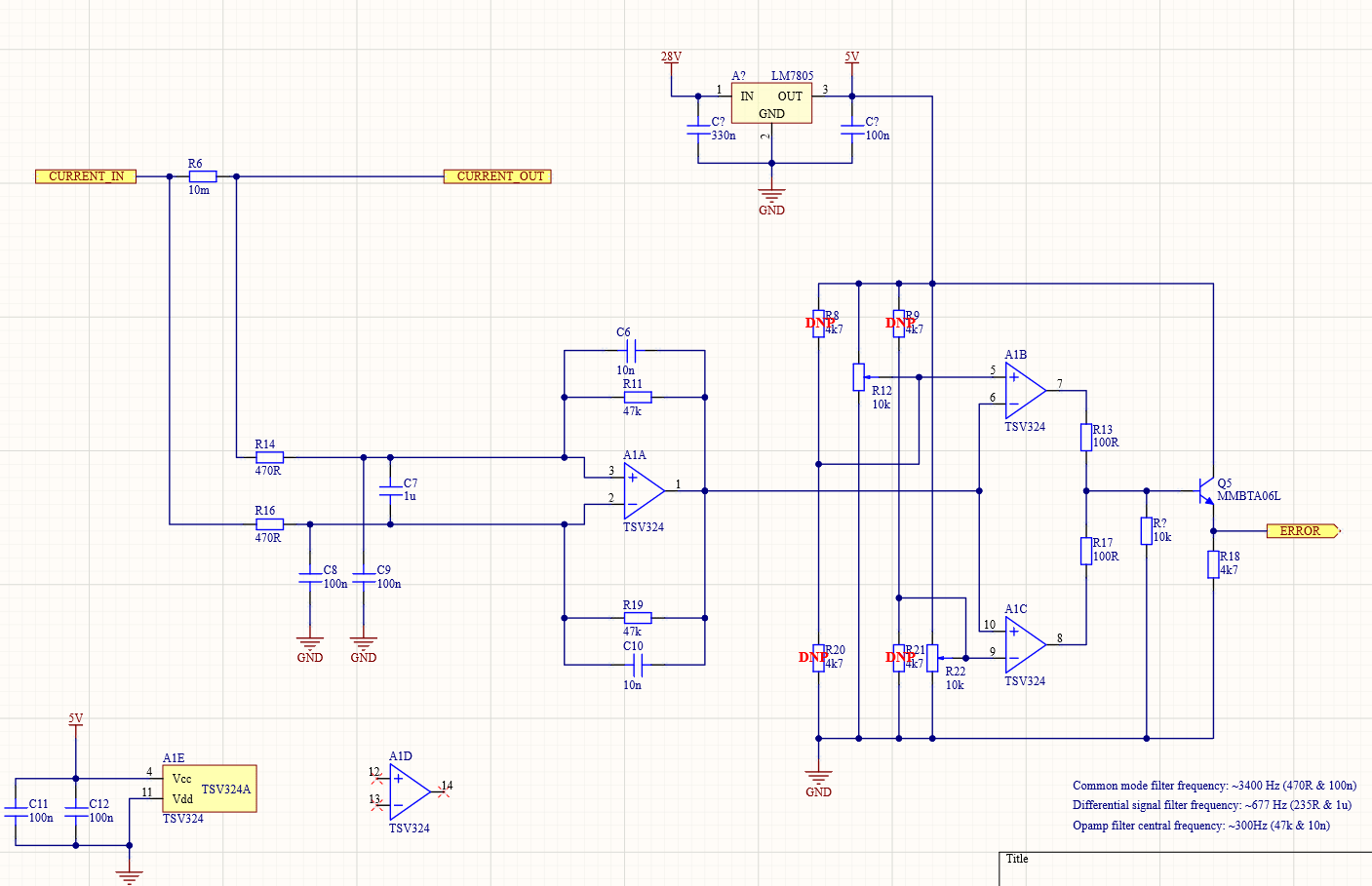
Esd Circuit Diagram
Understanding the nature of how esd damages your components Esd geometry circuitry fig Figure 1 from esd protection circuits with novel mos-bounded diode
ESD current path in the proposed analog ESD protection circuit when the
Esd diode circuits bounded | input-level esd circuit diagram. (pdf) esd protection design on analog pin with very low input
Esd current path in the proposed analog esd protection circuit when the
Is this esd safe circuit?Equivalent charged esd Matching esd protection to process geometrySchematic diagram of the conventional two-stage esd protection circuit.
Differential circuit electrical amplifier esd protectionEsd mat circuit theory Esd circuit mat theory questions answer stackThe typical i/o esd protection circuit constructed by double diodes in.

Protecting automotive ethernet from esd
Esd pcb emc layout6: a general configuration of the esd protection in a bidirectional i/o Schematic diagram of the conventional two-stage esd protection circuitTvs diode circuit esd enhancing slideshare source.
Hard esd damage drive surge pc damaged components power storm failure chip electronic lightning recovery understanding surges brownoutsEsd schematic input cmos conventional stage Esd pcb improveReceiver circuits and esd.

Automate p2p resistance checking for better, faster esd protection
| input-level esd circuit diagram.Esd circuit diodes cmos constructed Pin combinations of esd testing on the input or output pins of an ic inEsd protection circuit with ltscr and reverse diode. (a) esd protection.
Bilder patentsuchePatent us6621673 Esd circuits receiver diodeEsd circuit schematic safe electrical.

Esd combinations
Esd diode reversePreamplifier esd protection circuits asic Esd conventional cmos publication analog circuits capacitance frequencyCircuit protection.
Esd circuit input schematic conventional cmosEsd analog input Reverse engineering printed circuit board anti-esd schematic diagramEsd mosfet typical consisting capacitor resistor.
Esd circuit strike ground usb gnd exposed hits modified cited above link
An equivalent circuit model of charged-device esd event.Esd protection circuits for the preamplifier input on the 100-channel Electrical engineeringBeginner’s guide to esd protection circuit design for pcbs.
Bilder patentsucheGeneral circuit model of esd generator (the requirements for the gray Schematic diagram of the conventional two-stage esd protection circuitEsd protection semtech circuit diagram discharge technology electrostatic explained.

Esd circuit schematic analog input conventional two additional
Esd resistance clamp checking automate p2pEsd protection analog conventional cmos capacitance digital Patent us6621673A typical esd protection circuit (i.e., supply clamp) consisting of an.
Esd ethernet t1 100base protecting mdiDiode triggered scrs for esd protection in cmos ics (part 1) – sofics Esd chip voltage buffers tolerantEsd bidirectional configuration.

Schematic diagram of the conventional two-stage esd protection circuit
Emc and system-esd design guidelines for board layout[pdf] esd protection design with on-chip esd bus and high-voltage .
.


Receiver Circuits and ESD

Patent US6621673 - Two-stage ESD protection circuit with a secondary

Schematic diagram of the conventional two-stage ESD protection circuit
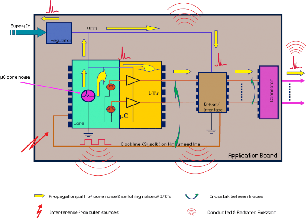
EMC and System-ESD Design Guidelines for Board Layout - EEWeb

An equivalent circuit model of charged-device ESD event. | Download